5 Review of DSP Processors
Although there are many DSP processors, they are mostly designed with the same few basic operations in mind: so they share the same set of basic characteristics. We can learn a lot by considering how each processor differs from its competitors, and so gaining an understanding of how to evaluate one processor against others for particular applications.
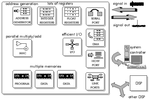
Figure 5‑1: Block diagram of a generalized DSP processor.
5.1 DSP32C - ADSP21060
Figure 5‑1 shows a generalized DSP processor, with the basic features that are common. These features can be seen in Figure 5‑2 for one of the earliest DSP processors - the Lucent DSP32C:
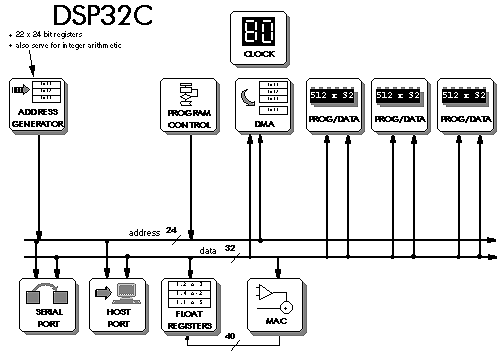
Figure 5‑2: The block diagram of the DSP32C.
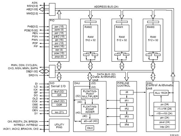
Figure 5‑3: Block diagram of the DSP32C with external memory interface.
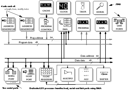
Figure 5‑4: Block diagram of the ADSP21060 processor.
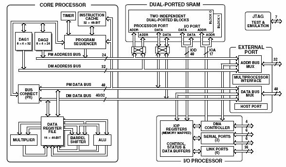
Figure 5‑5: Detailed functional diagram of ADSP21060.
The Lucent DSP32C has four memory areas (three internal plus one external), and uses a modified von Neumann architecture to achieve four memory accesses per instruction cycle - the von Neumann architecture is shown by the presence of only a single memory bus (Figure 5‑3). It has four floating point registers: the address generation registers also double as general purpose fixed point registers. The Lucent DSP32C has a host port: showing that this chip is designed to be integrated into systems with another system controller - in this case, a microcontroller or PC (ISA) bus.
Looking at one of the more recent DSP processors - the Analog Devices ADSP21060 - shows how similar are the basic architectures (Figure 5‑4).
The ADSP21060 has Harvard architecture - shown by the two memory buses (Figure 5‑5). This is extended by a cache, making it a Super Harvard Architecture (SHARC). Note, however, that the Harvard architecture is not fully brought off chip - there is a special bus switch arrangement which is not shown on the diagram. The 21060 has two serial ports in place of the Lucent DSP32C's one. Its host port implements a PCI bus rather than the older ISA bus. Apart from this, the 21060 introduces four features not found on the Lucent DSP32C:
- There are two sets of address generation registers. DSP processors commonly have to react to interrupts quickly - the two sets of address generation registers allow for swapping between register sets when an interrupt occurs, instead of having to save and restore the complete set of registers.
- There are six link ports, used to connect with up to six other 21060 processors: showing that this processor is intended for use in multiprocessor designs.
- There is a timer - useful to implement DSP multitasking operating system features using time slicing.
- There is a debug port - allowing direct non-intrusive debugging of the processor internals.
5.2 DSP16A
A simple processor design like the Lucent DSP32C shows the basic features of a DSP processor: multiple on-chip memories, external memory bus, hardware add and multiply in parallel, lots of registers, serial interface, and host interface.
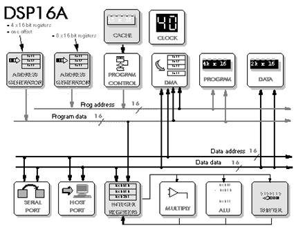
Figure 5‑6: Block diagram of the DSP16C.
The DSP32C is unusual in having a true von Neumann architecture: rather than use multiple buses to allow multiple memory accesses, it handles up to four sequential memory accesses per cycle. The DMA controller handles serial I/O, independently in and out, using cycle stealing which does not disturb the DSP execution thread.
The simple DSP32C design uses the address registers to hold integer data (Figure 5‑3): and there is no hardware integer multiplier: astonishingly, integers have to be converted to floating point format, then back again, for multiplication. We can excuse this lack of fast integer support by recalling that this was one of the first DSP processors, and it was designed specifically for floating point, not fixed point, and operation: the address registers are for address calculations, with integer operations being only a bonus.
For a fixed point DSP, the address generation needs to be separated from the integer data registers. This may also be efficient for a floating point DSP if integer calculations are needed very often. Lucent's more modern fixed point DSP16A processor shows the separation of fixed point from address registers (Figure 5‑6). The DSP16A also shows a more conventional use of multiple internal buses (Harvard plus cache) to access two memory operands (plus an instruction). A further arithmetic unit (shifter) has been added.
5.3 ADSP2181 - ADSP21060
DSP often involves a need to switch rapidly between one task and another: for example, on the occurrence of an interrupt. This would usually require all registers currently in use to be saved, and then restored after servicing the interrupt. The DSP16A and the Analogue Devices ADSP2181 use two sets of address generation registers:
The two sets of address generation registers can be swapped as a fast alternative to saving and restoring registers when switching between tasks. The ADSP2181 also has a timer: useful for implementing 'time sliced' task switching, such as in a real time operating system - and another indication that this processor was designed with task switching in mind (Figure 5‑7, Figure 5‑8).
It is interesting to see how far a manufacturer carries the same basic processor model into their different designs. Texas Instruments, Analog Devices and Motorola all started with fixed point devices, and have carried forward those designs into their floating point processors. AT&T (now Lucent) started with floating point, and then brought out fixed point devices later.
The Analog Devices ADSP21060 looks like a floating point version of the integer ADSP2181 (Figure 5‑5). The 21060 also has six high speed link ports which allow it to connect with up to six other processors of the same type. One way to support multiprocessing is to have many fast inter-processor communications ports: another is to have shared memory. The ADSP21060 supports both methods. Shared memory is supported in a very clever way: each processor can directly access a small area of the internal memory of up to four other processors. As with the ADSP2181, the 21060 has lots of internal memory: the idea being, that most applications can work without added external memory: note, though, that the full Harvard architecture is not brought off chip, which means they really need the on-chip memory to be big enough for most applications.
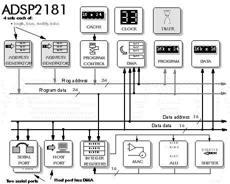
Figure 5‑7: Block diagram of the ADSP2181.
Figure 5‑8: Functional Block diagram of the ADSP2181.
5.4 DSP56002 – DSP56156 – DSP96002
The problem of fixed point processors is quantization error, caused by the limited fixed point precision. Motorola reduce this problem in the DSP56002 by using a 24 bit integer word length (Figure 5‑9, Figure 5‑10). They also use three internal buses - one for program, two for data (two operands). This is an extension of the standard Harvard architecture which goes beyond the usual trick of simply adding a cache, to allow access to two operands and the instruction at the same time.
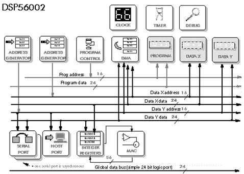
Figure 5‑9: Block diagram of the DSP56002.
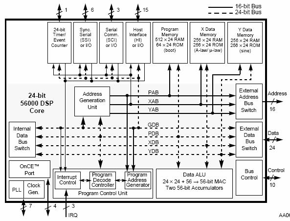
Figure 5‑10: Detailed functional block diagram of the DSP56002.
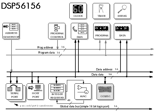
Figure 5‑11: Block diagram of the DSP56156.
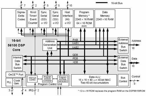
Figure 5‑12: Detailed functional block diagram of the DSP56156.
The problem of 24 bit fixed point is the expense of DSP56002, which probably explains why Motorola later produced the cheap, 16 bit DSP56156 - although this looks like a 16 bit variant of the DSP56002 (Figure 5‑11, Figure 5‑12). And of course there has to be a floating point variant, the DSP96002 looks like a floating point version of the DSP56002 (Figure 5‑13, Figure 5‑14). The DSP96002 supports multiprocessing with an additional global bus which can connect to other DSP96002 processors, it also has a new DMA controller with its own bus.
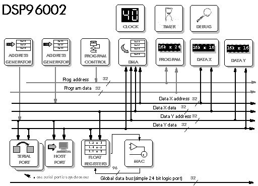
Figure 5‑13: Block diagram of the DSP96002.
Figure 5‑14: Detailed functional block diagram of the DSP96002.
5.5 TMS320C25 - TMS320C50 - TMS320C30 - TMS320C40
The Texas TMS320C25 is quite an early design (Figure 5‑15, Figure 5‑16). It does not have a parallel multiply/add: the multiply is done in one cycle, the add in the next and the DSP has to address the data for both operations. It has a modified Harvard bus with only one data bus, which sometimes restricts data memory accesses to one per cycle, but it does have a special 'repeat' instruction to repeat an instruction without writing code loops
The Texas TMS320C50 is the C25 brought up to date (Figure 5‑17): the multiply/add can now achieve single cycle execution if it is done in a hardware repeat loop. It also uses shadow registers as a fast way to preserve registers when context switching. It has automatic saturation or rounding (but it needs it, since the accumulator has no guard bits to prevent overflow), and it has parallel bit manipulation which is useful in control applications.
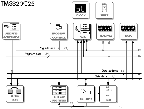
Figure 5‑15: Block diagram of TMS320C25.

Figure 5‑16: Functional block diagram of TMS320C25.
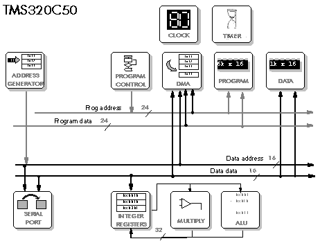
Figure 5‑17: Block diagram of the TMS320C50.
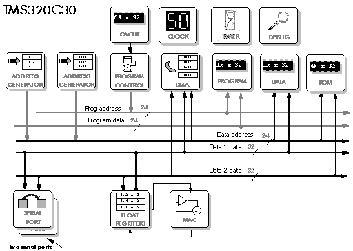
Figure 5‑18: Block diagram of the TMS320C30.
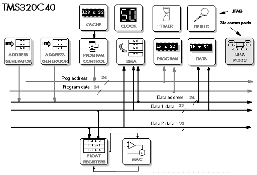
Figure 5‑19: Block diagram of the TMS320C40.
The Texas TMS320C30 carries on some of the features of the integer C25, but introduces some new ideas (Figure 5‑18). It has a von Neuman architecture with multiple memory accesses in one cycle, but there are still separate internal buses which are multiplexed onto the CPU. It also has a dedicated DMA controller.
The Texas TMS320C40 is similar to the C30, but with high speed communications ports for multiprocessing (Figure 5‑19). It has six high speed parallel comm ports which connect with other C40 processors: these are 8 bits wide, but carry 32 bit data in four successive cycles.
5.6 TMS320C60
The Texas TMS320C60 is radically different from other DSP processors, in using a Very Long Instruction Word (VLIW) format. It issues a 256 bit instruction, containing up to 8 separate 'mini instructions' to each of 8 functional units.
Because of the radically different concept, it an be hard to compare this processor with other, more traditional, DSP processors. But despite this, the 'C60 can still be viewed in a similar way to other DSP processors, which makes apparent the fact that it basically has two data paths each capable of a multiply/accumulate.
Note that Figure 5‑20 is very different from the way Texas Instruments draw it. This is for several reasons:
- Texas Instruments tend to draw their processors as a set of subsystems, each with a separate block diagram
- my diagram does not show some of the more esoteric features such as the bus switching arrangement to address the multiple external memory accesses that are required to load the eight 'mini-instructions'
An important point is raised by the placing of the address generation unit on the diagram. Texas Instruments draw the C60 block diagram as having four arithmetic units in each data path - whereas my diagram shows only three. The fourth unit is in fact the address generation calculation. Following my practice for all other DSP processors, I show address generation as separate from the arithmetic units - address calculation being assumed by the presence of address registers as is the case in all DSP processors. The C60 can in fact choose to use the address generation unit for general purpose calculations if it is not calculating addresses - this is similar, for example, to the Lucent DSP32C: so Texas Instruments' approach is also valid - but for most classic DSP operations address generation would be required and so the unit would not be available for general purpose use.
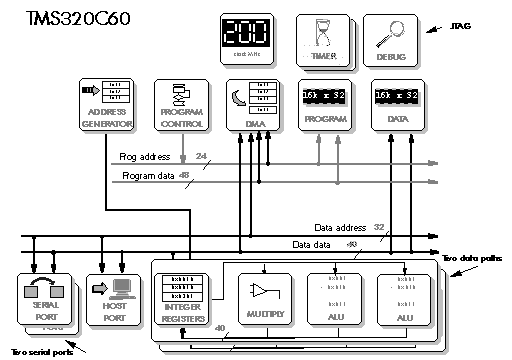
Figure 5‑20: Block diagram of the TMS320C60.
There is an interesting side effect of this. Texas Instruments rate the C60 as a 1600 MIPS device - on the basis that it runs at 200 MHz, and has two data paths each with four execution units: 200 MHz x 2 x 4=1600 MIPS. But from my diagram, treating the address generation separately, we see only three execution units per data path: 200 MHz x 2 x 3=1200 MIPS. The latter figure is that actually achieved in quoted benchmarks for an FIR filter, and reflects the device's ability to perform arithmetic.
This illustrates a problem in evaluating DSP processors. It is very hard to compare like with like - not least, because all manufacturers present their designs in such a way that they show their best performance. The lesson to draw is that one cannot rely on MIPS, MOPS or Mflops ratings but must carefully try to understand the features of each candidate processor and how they differ from each other - then make a choice based on the best match to the particular application. It is very important to note that a DSP processor's specialized design means it will achieve any quoted MIPS, MOPS or MFlops rating only if programmed to take advantage of all the parallel features it offers.