4 Memory Architectures
DSP processor data paths are optimized to provide extremely high performance on certain kinds of arithmetic-intensive algorithms. However, a powerful data path is, at best, only part of a high-performance processor. To keep the data path fed with data and to store the results of data path operations, DSP processors require the ability to move large amounts of data to and from memory quickly.
DSP processor data paths are designed to perform a multiply-accumulate operation in one instruction cycle. This means that the arithmetic operations required for one tap can be computed in one instruction cycle. However, to achieve this performance, the processor must be able to make several accesses to memory within one instruction cycle. Specifically, the processor must:
- fetch the multiply-accumulate instruction,
- read the appropriate data value from the delay line,
- read the appropriate coefficient value, and
- write the data value to the next location in the delay line to shift data through the delay line.
Thus, the processor must make four accesses to memory in one instruction cycle if the multiply-accumulate operation is to execute in a single instruction cycle. In practice, some processors use other techniques (as discussed later) to reduce the actual number of memory accesses needed to three or even two. Nevertheless, all processors require multiple memory accesses within one instruction cycle. This level of memory bandwidth is needed for many important DSP algorithms.
4.1 Features for Reducing Memory Access Requirements
Some DSP processors provide special features designed to reduce the number of memory accesses required to perform certain kinds of operations. Under some circumstances these features allow such processors to achieve equal performance to other processors that provide more memory bandwidth. Because a processor with more memory bandwidth is generally more expensive, features that reduce memory access requirements also tend to reduce processor cost. Of course, they may also increase execution time or software development time, and therefore represent a trade-off that must be carefully considered by the system designer.
4.1.1 Program Caches
Some DSP processors incorporate a program cache, which is a small memory within the processor core that is used for storing program instructions to eliminate the need to access program memory when fetching certain instructions. Avoiding a program instruction fetch can free up a memory access to be used for a data read or write, or it can speed operation by avoiding delays associated with slow external (off-chip) program memory.
DSP processor caches vary significantly in their operation and capacity. They are generally much smaller and simpler than the caches associated with general-purpose microprocessors. We briefly discuss each of the major types of DSP processor caches below.
The simplest type of DSP processor cache is a single-instruction repeat buffer. This is a one-word instruction cache that is used with a special repeat instruction. A single instruction that is to be executed multiple times is loaded into the buffer upon its first execution; immediately subsequent executions of the same instruction fetch the instruction from the cache, freeing the program memory to be used for a data read or write access. For example, the Texas Instruments TMS320C2x and TMS320C5x families provide one program memory access and one data memory access per instruction cycle. However, when an instruction is placed in the repeat buffer for repeated execution, the second and subsequent executions of the instruction can perform two memory accesses (one to program memory to fetch one data value and one to data memory to fetch another data value). Thus, when the repeat instruction is used, the processor can achieve performance comparable to a processor that provides three memory accesses per instruction cycle. The obvious disadvantage to the repeat buffer approach is that it only works on one instruction at a time, and that instruction must be executed repeatedly. While this is very useful for some algorithms (e.g., dot-product computation), it does not help for algorithms in which a block of multiple instructions must be executed repeatedly as a group.
The repeat buffer concept can be extended to accommodate more than one program instruction. For example, the AT&T DSP16xx provides a 16-entry repeat buffer. The DSP16xx buffer is loaded when the programmer specifies a block of code of 16 or fewer words to be repeated using the repeat instruction. The first time through, the block of instructions are read from program memory and copied to the buffer as they are executed. During each repetition, the instructions are read from the buffer, freeing one additional memory access for a data read or write. As with the TMS320C2x and TMS320C5x, the DSP16xx can achieve two data transfers per instruction cycle when the repeat buffer is used. Multi-word repeat buffers work well for algorithms that contain loops consisting of a modest number of instructions. This type of loop is quite common in DSP algorithms, since many (if not most) DSP algorithms contain groups of several instructions that are executed repeatedly. Such loops are often used in filtering, transforms, and block data moves.
A generalization of the multi-instruction repeat buffer is a simple single-sector instruction cache. This is a cache that stores some number of the most recent instructions that have been executed. If the program flow of control jumps back to an instruction that is in cache (a cache hit), the instruction is executed from the cache instead of being loaded from program memory. This frees up an additional memory access for a data transfer, and avoids a speed penalty that may be associated with accessing slow off-chip program memory. The limitation on this type of cache is that it can only be used to access a single, contiguous region of program memory. When a program control flow change (for example, a branch instruction or an interrupt service routine) accesses a program memory location that is not already contained in the cache, the previous contents of the cache are invalidated and cannot be used.
The difference between the single-sector instruction cache and the multi-word repeat buffer is that the cache is loaded with each instruction as it is executed and tracks the addresses of the instructions in the cache. If the program flow of control jumps to a program address that is contained in the cache, the processor detects this and accesses the instructions out of the cache. This means that the cache can be accessed by variety of instructions, such as jump, return, etc. With the repeat buffer, only the repeat instruction can be used to access instructions in the cache. This means that a repeat buffer cannot be used to hold branch instructions. An example of a processor using a single-sector cache is the Zoran ZR3800x. As with multi-word repeat buffers, single-sector caches are useful for a wide range of DSP processor operations that involve repetitively executing small groups of instructions.
A more flexible structure is a cache with multiple independent sectors. This type of cache functions like the simple single-sector instruction cache, except that two or more independent segments of program memory can be stored. For example, the cache in the Texas Instruments TMS320C3x contains two sectors of 32 words each. Each sector can be used to store instructions from an independent 32-word region of program memory. If the processor attempts to fetch an instruction from an external memory location that is stored in the cache (a cache hit), the external access is not made, and the word is taken from the cache. If the memory location is not in the cache (a 1cache miss), then the instruction is fetched from external memory, and the cache is updated in one of two ways. If the external address was from one of the two 32-word sectors currently associated with the cache, then the word is stored in the cache at the appropriate location within that sector. If the external address does not fall within the two 32-word sectors currently being monitored by the cache, then a sector miss occurs. In this case, the entire contents of one of the sectors are discarded and that sector becomes associated with the 32-word region of memory containing the accessed address. In the case of Texas Instruments processors, the algorithm used to determine which cache sector should be discarded when a sector miss occurs is the least-recently-used (or LRU) algorithm. This algorithm keeps track of when each cache sector has been accessed. When a cache sector is needed to load new program memory locations, the algorithm selects the cache sector that has not been read from for the longest time.
Some DSP processors with instruction caches provide special instructions or configuration bits that allow the programmer to lock the contents of the cache at some point during program execution or to disable the cache altogether. These features provide a measure of manual control over cache mechanisms, which may allow the programmer to obtain better performance than would be achieved with the built-in cache management logic of the processor. In addition, imposing manual control over cache loading may help software developers to ensure that their code will meet critical real-time constraints.
An interesting approach to caches was introduced by Motorola with the updated DSP96002. This processor allows the internal 1 Kword by 32-bit program memory to be configured either as an instruction cache or as program memory. When the cache is enabled, it is organized into eight 128-word sectors. Each sector can be individually locked and unlocked. Motorola's more recent DSP563xx family includes a similar dual cache/memory construct.
A variation on the multi-sector caches just discussed is the Analog Devices ADSP-210xx cache. The ADSP-210xx uses a two-bank Harvard architecture; instructions that access data from program memory require two accesses and therefore cause contention for program memory. Because the ADSP-210xx cache is only loaded with instructions whose execution causes contention for program memory access, the cache is more efficient than a traditional cache, which stores every instruction fetched.
Although DSP processor caches are in some cases beginning to approach the sophistication of caches found in high-performance general-purpose processors, there are still some important differences. In particular, DSP processor caches are only used for program instructions, not for data. A cache that accommodates data as well as instructions must include a mechanism for updating both the cache and external memory when a data value held in the cache is modified by the program. This adds significantly to the complexity of the cache hardware.
4.1.2 Modulo Addressing
Cache memories reduce the number of accesses to a processor's main memory banks required to accomplish certain operations. They do this by acting as an additional, specialized memory bank. In special circumstances, it is possible to use other techniques to reduce the number of total memory accesses (including use of a cache, if one exists) required to accomplish certain operations. One such technique is modulo addressing. Modulo addressing enables a processor to implement a delay line, without actually having to move the data values in memory. Instead, data values are written to one memory location and remain there until they are no longer needed. The effect of data shifting along a delay line is simulated by manipulating memory pointers using modulo arithmetic. This technique reduces the number of simultaneous memory accesses required to implement the FIR filter example from four per instruction cycle to three per instruction cycle.
4.2 Wait States
As the name implies, wait states are states in which the processor cannot execute its program because it is waiting for access to memory. Wait states occur for three reasons: contention, slow memory, and bus sharing.
Conflict wait states occur when the processor attempts to make multiple simultaneous accesses to a memory that cannot accommodate multiple accesses. This may occur, for example, when a single bank of single-access memory contains both instruction words and data. Since most DSP processors are heavily pipelined, the execution of a single instruction is often spread across several instruction cycles. Therefore, conflict wait states can arise even when a particular single instruction does not require more accesses to a given memory bank than that memory bank can support, because adjacent instructions may require memory access at the same time.
Almost all processors recognize the need for conflict wait states and automatically insert the minimum number of conflict wait states needed. Exceptions to this are a few members of the AT&T DSP16xx family (the DSP1604, DSP1605, and DSP1616). On these processors, attempting to fetch words from both external program and data memory in one instruction cycle results in a correct program word fetch, but the fetched data word is invalid.
Most DSP processors include one or more small banks of fast on-chip RAM and/or ROM that provide one or more accesses per instruction cycle. In many situations, it is necessary or desirable to expand this memory using off-chip memory that is too slow to support a complete memory access within one processor instruction cycle. Typically this is done to save cost, since slower memory chips are cheaper than faster ones. In these cases, the processor is configured to insert programmed wait states during external memory accesses. These wait states are configured by the programmer to deliberately slow down the processor's memory accesses to match the speed of slow memories. Some processors can be programmed to use different numbers of programmed wait states when accessing different regions of off-chip memory, so cost-effective combinations of slower and faster memory can be used.
In some systems, it may not be possible to predict in advance precisely how many wait states will be required to access external memory. For example, when the processor shares an external memory bus with one or more other processors, the processor may have to wait for another processor to relinquish the bus before it can proceed with its own access. Similarly, if dynamic memory (DRAM) is used, the processor may have to wait while the DRAM controller refreshes the DRAM. In these cases, the processor must have the ability to dynamically insert externally requested wait states until it receives a signal from an external bus or memory controller that the external memory is ready to complete the access. For example, the Texas Instruments TMS320C5x provides a special READY pin that can be used by external hardware to signal the processor that it must wait before continuing with an external memory access.
The length of a wait state relative to the length of a processor instruction cycle varies from processor to processor. Wait state lengths typically range from one quarter of an instruction cycle (as on the AT&T DSP32C) to a full instruction cycle (as on most processors). Shorter wait states allow more efficient operation, since the delay from the time when the external memory is ready for an access to the time when the wait state ends and the processor begins the access will likely be shorter.
4.3 ROM
DSP processors that are intended for low-cost, embedded applications like consumer electronics and telecommunications equipment provide on-chip read-only memory (ROM) to store the application program and constant data. Some manufacturers offer multiple versions of their processors: a version with internal RAM for prototyping and for low-volume production, and a version with factory-programmed ROM for large-volume production. On-chip ROM sizes typically range from 256 words to 36 Kwords.
Texas Instruments offers versions of some of its processors (e.g., the TMS320P17 and TMS320P25) with one-time-programmable ROM on-chip. These devices can be programmed by the system manufacturer using inexpensive PROM programmers, either for prototyping or for low- or medium-volume production.
For applications requiring more ROM than is provided on-chip by the chosen processor, external ROM can be connected to the processor through its external memory interface. Typically, multiple ROM chips are used to create a bank of memory whose width matches the width of the program word of the processor. However, some processors have the ability to read their initial (boot) program from an inexpensive byte-wide external ROM. These processors construct instruction words of the appropriate width by concatenating bytes from the ROM.
4.4 External Memory Interfaces
DSP processors' external memory interfaces differ in three main features: number of memory ports, sophistication and flexibility of the interface, and timing requirements.
Most DSP processors provide a single external memory port consisting of an address bus, a data bus, and a set of control signals, even though most DSP processors have multiple independent memory banks on-chip. This is because extending buses off-chip requires large numbers of package pins, which increase the cost of the processor. Most processors with multiple on-chip memory banks provide the flexibility to use the external memory port to extend any of the internal memory banks off-chip. However, the lack of multiple external memory ports usually means that multiple accesses cannot be made to external memory locations within a single instruction cycle, and programs attempting to do so will incur a performance penalty. Figure 4‑1 illustrates a typical DSP processor external memory interface, with three independent sets of on-chip memory buses sharing one external memory interface.
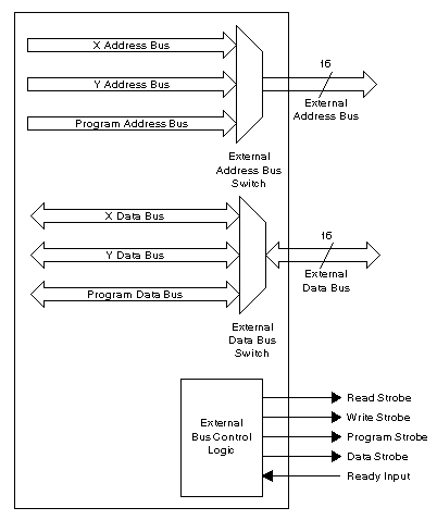
Figure 4‑1:
Example DSP processor
external memory interface. The processor has
three sets of on-chip memory buses, but only one set of off-chip memory buses.
The on-chip buses are multiplexed such that any one of the on-chip bus sets can
be
connected to the off-chip bus set.
Some DSP processors do provide multiple off-chip memory ports. The Analog Devices ADSP-21020 provides an external program memory port (24-bit address, 48-bit data) and an external data memory port (32-bit address, 32-bit data). The Texas Instruments TMS320C30 provides one 24-bit address, 32-bit data external memory port, and one 13-bit address, 32-bit data external memory port, while the TMS320C40 has two identical 31-bit addresses, 32-bit data external memory ports. Similarly, the Motorola DSP96002 provides two identical 32-bit address and data bus sets. The cost of these devices is correspondingly higher than that of comparable processors with only one external memory port.
DSP processor external memory interfaces vary quite a bit in flexibility and sophistication. Some are relatively simple and straightforward, with only a handful of control pins. Others are much more complex, providing the flexibility to interface with a wider range of external memory devices and buses without special interfacing hardware. Some of the features distinguishing external memory interfaces are the flexibility and granularity of programmable wait states, the inclusion of a wait pin to signal the availability of external memory, bus request and bus grant pins (discussed below), and support for page-mode DRAM (discussed below).
High-performance applications must often use fast static RAM devices for off-chip memory. In such situations, it is important for system hardware designers to scrutinize the timing specifications for DSP processors' external memory ports. Because timing specifications can vary significantly among processors, it is common to find two processors that have the same instruction cycle time but have very different timing specifications for off-chip memory. These differences can have a serious impact on system cost, because faster memories are significantly more expensive than slower memories. Hardware design flexibility is also affected, since more stringent timing specifications may constrain the hardware designer in terms of how the interface circuitry is designed and physically laid out.
4.4.1 Manual Caching
Whether or not a processor contains a cache, it is often possible for software developers to improve performance by explicitly copying sections of program code from slower or more congested (in terms of accesses) memory to faster or less congested memory. For example, if a section of often-used program code is stored in a slow, off-chip ROM, then it may make sense to copy that code to faster on-chip RAM, either at system start-up or when that particular program section is needed.
4.5 Multiprocessor Support in External Memory Interfaces
Interfaces DSP processors intended for use in multiprocessor systems often provide special features in their external memory interfaces to simplify the design and enhance the performance of such systems. The first and most obvious of these features is the provision of two external memory ports, mentioned above. The availability of two external memory ports means that one port can be connected to a local, private memory, while the other is connected to a memory shared with other processors. For example, the Motorola DSP96002 includes two external memory ports expressly for use in such multiprocessor configurations.
When a multiprocessor system includes two or more processors that share a single external memory bus, a mechanism must be provided for the processors to negotiate control of the bus (bus arbitration) and to prevent the processors that do not have control of the bus from trying to assert values onto the bus. Several DSP processors provide features to facilitate this kind of arrangement, though there are significant differences in the sophistication and flexibility of the features provided. In some cases, a shared bus multiprocessor can be created simply by connecting together the appropriate pins of the processors without the need for any special software or hardware to manage bus arbitration. In other cases, extra software on one or more of the DSP processors and/or external bus arbitration hardware may be required.
An example of basic support for shared bus systems is provided by the Motorola DSP5600x. Two of the DSP processor's pins can be configured to act as bus request and bus grant signals. When an external bus arbitrator (either another processor or dedicated hardware) wants a particular DSP processor to relinquish the shared bus, it asserts that processor's bus request input. The processor then completes any external memory access in progress and relinquishes the bus, acknowledging with the bus grant signal that it has done so. The DSP processor can continue to execute its program as long as no access to the shared bus is required. If an access to the shared bus is required, the processor waits until the bus request signal has been de-asserted, indicating that it can again use the shared bus.
The Texas Instruments TMS320C5x provides several features that support multiprocessing. In addition to providing the equivalent of bus request and bus grant signals (called HOLD and HOLDA on the TMS320C5x), the processor also allows an external device to access its on-chip memory. To accomplish this, the external device first asserts the TMS320C5x's HOLD input. When the processor responds by asserting HOLDA, the external device asserts BR, indicating that it wishes to access the TMS320C5x's on-chip memory. The TMS320C5x responds by asserting IAQ. The external device can then read and write the TMS320C5x's on-chip memory by driving TMS320C5x's address, data, and read/write lines. When finished, the external device deasserts HOLD and BR. This allows the creation of multiprocessor systems that do not require shared memory for interprocessor communications.
A processor feature that simplifies the use of shared variables in shared memory is bus locking, which allows a processor to read the value of a variable from memory, modify it, and write the new value back to memory, while ensuring that this sequence of operations is not interrupted by another processor attempting to update the variable's value. This is sometimes referred to as an atomic test-and-set operation. The Texas Instruments TMS320C3x and TMS320C4x processors provide special instructions and hardware support for bus locking; Texas Instruments refers to these operations as "interlocked operations."
The Analog Devices ADSP-2106x offers a sophisticated shared bus interface. The processor provides on-chip bus arbitration logic that allows direct interconnection of up to six ADSP-2106x devices with no special software or external hardware required for bus arbitration. In addition, the processor allows one DSP processor in a shared-bus configuration to access another processor's on-chip memory, much like on the Texas Instruments TMS320C5x family. This means that inter-processor data moves will not necessarily have to transit through an external shared memory.
In addition to special external memory interface features, the Analog Devices ADSP-2106x and the Texas Instruments TMS320C4x families provide special communications ports to facilitate connections within multiprocessor systems.
4.5.1 Dynamic Memory
All of the writable memory found on DSP processors and most of the memory found in systems based on DSP processors is static memory, also called SRAM (for static random-access memory; a better name would have been static read and write memory). Static memory is simpler to use and faster than dynamic memory (DRAM), but it also requires more silicon area and is more costly for a given number of bits of memory. The key operational attribute distinguishing static from dynamic memories is that static memories retain their data as long as power is available. Dynamic memories must be refreshed periodically; that is, a special sequence of signals must be applied to reinforce the stored data, or it eventually (typically in a few tens of milliseconds) is lost. In addition, interfacing to static memories is usually simpler than interfacing to dynamic memories; the use of dynamic memories usually requires a separate, external DRAM controller to generate the necessary control signals.
Because of the increasing proliferation of DSP processors into low-cost, high-volume products like answering machines and personal computer add-in cards, there has been increased interest in using dynamic memory in DSP systems. DRAM can also be attractive for systems that require large quantities of memory, such as large-scale multiprocessor systems.
One way to get faster, static RAM-like performance from slower, dynamic RAM is the use of paged or static column DRAM. These are special types of DRAM chips that allow faster than normal access when a group of memory accesses occur within the same region (or page) of memory. Some DSP processors, including the Motorola DSP96002, the Analog Devices ADSP-210xx, and the Texas Instruments TMS320C3x and TMS320C4x provide memory page boundary detection capabilities. These capabilities generally consist of a set of programmable registers, which the programmer uses to specify the locations of page boundaries in external memory, and circuitry to detect when external memory accesses cross page boundaries. In most cases, when the processor detects that a memory access has crossed a page boundary, it asserts a special output pin. It is then up to the external DRAM controller to use a processor input pin to signal back to the processor that it must delay its access by inserting wait states while the controller readies the DRAM for access to a new page.
As mentioned above, the use of DRAM as external memory for a DSP processor usually requires the use of an external DRAM controller chip. This additional chip may increase the manufacturing cost of the design, which partly defeats the reason for using DRAM in the first place. To address this problem, some DSP processors now incorporate a DRAM controller on-chip. The Motorola DSP56004 and DSP56007, for example, provide on-chip DRAM interfaces that include support for page-mode DRAM.
4.5.2 Direct Memory Access
Direct memory access (DMA) is a technique whereby data can be transferred to or from the processor's memory without the involvement of the processor itself. DMA is typically used to provide improved performance for input/output devices. Rather than have the processor read data from an I/O device and copy the data into memory or vice versa, a separate DMA controller can handle such transfers more efficiently. This DMA controller may be a peripheral on the DSP chip itself or it may be implemented using external hardware.
Any processor that has the simple bus request/bus grant mechanism described above can be used with an external DMA controller that accesses external memory. Typically the processor loads the DMA controller with control information including the starting memory address for the transfer, the number of data words to be transferred, the direction of the transfer, and the source or destination peripheral. The DMA controller uses the bus request pin to notify the DSP processor that it is ready to make a transfer to or from external memory. The DSP processor completes its current instruction, relinquishes control of external memory, and signals the DMA controller via the bus grant pin that the DMA transfer can proceed. The DMA controller then transfers the specified number of data words and optionally signals completion to the processor through an interrupt.
Some more sophisticated DSP processors include a DMA controller on-chip that can access internal and external memory. These DMA controllers vary in their performance and flexibility. In some cases, the processor's available memory bandwidth may be large enough to allow DMA transfers to occur in parallel with normal program instruction and data transfers without any impact on performance. For example, the Texas Instruments TMS320C4x contains a DMA controller that, combined with the TMS320C4x's on-chip memory and on-chip DMA address and data buses, can complete one memory access per instruction cycle independent of the processor. The Motorola DSP96002, the Texas Instruments TMS320C3x family, and the Analog Devices ADSP-2106x family all include on-chip DMA controllers with similar capabilities.
Some DMA controllers can manage multiple DMA transfers in parallel. Such a DMA controller is said to have multiple channels, each of which can manage one transfer, and each of which has its own set of control registers. The TMS320C4x DMA controller supports six channels, the Analog Devices ADSP-2106x supports ten channels, and the Motorola DSP96002 can handle two channels. Each channel can be used for memory-memory or memory-peripheral transfers.
In contrast, the AT&T DSP3210 includes a more limited, two-channel DMA controller that can only be used for transfers to and from the processor's internal serial port. Since the DSP3210 does not have extra memory bandwidth, the currently executing instruction is forced to wait one cycle when the DMA controller accesses memory. This arrangement (where the processor is suspended during DMA bus accesses) is called cycle stealing. The Analog Devices ADSP-21xx provides a similar capability through a mechanism that Analog Devices calls auto buffering.