3 Introduction to Digital Signal Processors
3.1 How DSPs are Different from Other Microprocessors
The last forty years have shown that computers are extremely capable in two broad areas, data manipulation, such as word processing and database management, and mathematical calculation, used in science, engineering, and Digital Signal Processing. All microprocessors can perform both tasks; however, it is difficult (expensive) to make a device that is optimized for both. There are technical tradeoffs in the hardware design, such as the size of the instruction set and how interrupts are handled. Even more important, there are marketing issues involved: development and manufacturing cost, competitive position, product lifetime, and so on. As a broad generalization, these factors have made traditional microprocessors, such as the Pentium, primarily directed at data manipulation. Similarly, DSPs are designed to perform the mathematical calculations needed in Digital Signal Processing.
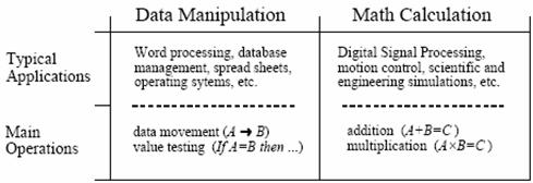
Figure 3‑1: Data manipulation versus mathematical calculation.
Figure 3‑1 lists the most important differences between these two categories. Data manipulation involves storing and sorting information. For instance, consider a word processing program. The basic task is to store the information (typed in by the operator), organize the information (cut and paste, spell checking, page layout, etc.), and then retrieve the information (such as saving the document on a floppy disk or printing it with a laser printer). These tasks are accomplished by moving data from one location to another, and testing for inequalities (A=B, A<B, etc.). As an example, imagine sorting a list of words into alphabetical order. Each word is represented by an 8 bit number, the ASCII value of the first letter in the word. Alphabetizing involved rearranging the order of the words until the ASCII values continually increase from the beginning to the end of the list. This can be accomplished by repeating two steps over-and-over until the alphabetization is complete. First, test two adjacent entries for being in alphabetical order (IF A>B THEN ...). Second, if the two entries are not in alphabetical order, switch them so that they are (A«B). When this two-step process is repeated many times on all adjacent pairs, the list will eventually become alphabetized.
As another example, consider how a document is printed from a word processor. The computer continually tests the input device (mouse or keyboard) for the binary code that indicates, "print the document." When this code is detected, the program moves the data from the computer's memory to the printer. Here we have the same two basic operations: moving data and inequality testing. While mathematics is occasionally used in this type of application, it is infrequent and does not significantly affect the overall execution speed.
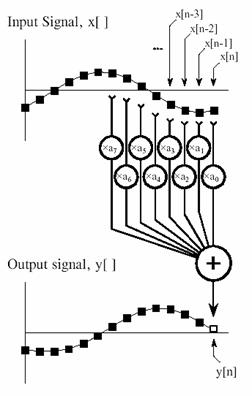
Figure 3‑2: FIR digital filter. Each sample in the output signal is found by multiplying samples from the input signal by the kernel coefficients and summing the products.
In comparison, the execution speed of most DSP algorithms is limited almost completely by the number of multiplications and additions required. For example, Figure 3‑2 shows the implementation of an FIR digital filter, the most common DSP technique. Using the standard notation, the input signal is referred to by x[ ], while the output signal is denoted by y[ ]. Our task is to calculate the sample at location n in the output signal. An FIR filter performs this calculation by multiplying appropriate samples from the input signal by a group of coefficients, denoted by a0, a1, a2, a3,…, and then adding the products. This is simply saying that the input signal has been convolved with a filter kernel consisting of a0, a1, a2, a3,…. Depending on a0, a1, a2, a3... the application, there may only be a few coefficients in the filter kernel, or many thousands. While there is some data transfer and inequality evaluation in this algorithm, such as to keep track of the intermediate results and control the loops, the math operations dominate the execution time.
In addition to performing mathematical calculations very rapidly, DSPs must also have a predictable execution time. Suppose you launch your desktop computer on some task, say, converting a word-processing document from one form to another. It does not matter if the processing takes ten milliseconds or ten seconds; you simply wait for the action to be completed before you give the computer its next assignment.
In comparison, most DSPs are used in applications where the processing is continuous, not having a defined start or end. For instance, consider an engineer designing a DSP system for an audio signal, such as a hearing aid. If the digital signal is being received at 20,000 samples per second, the DSP must be able to maintain a sustained throughput of 20,000 samples per second. However, there are important reasons not to make it any faster than necessary. As the speed increases, so does the cost, the power consumption, the design difficulty, and so on. This makes an accurate knowledge of the execution time critical for selecting the proper device, as well as the algorithms that can be applied.
3.2 Characteristics of DSP processors
Although there are many DSP processors, they are mostly designed with the same few basic operations in mind, that they share the same set of basic characteristics. These characteristics fall into three categories:
- SSpecialized high speed arithmetic
- DData transfer to and from the real world
- MMultiple access memory architectures
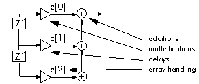
Figure 3‑3: Typical DSP operations require specific functions.
Typical DSP operations require a few specific operations. Figure 3‑3 shows an FIR filter and illustrates the basic DSP operations: additions and multiplications, delays, and array handling. Each of these operations has its own special set of requirements. Additions and multiplications require us to fetch two operands, perform the addition or multiplication (usually both), store the result, or hold it for a repetition. Delays require us to hold a value for later use. Array handling requires us to fetch values from consecutive memory locations, and copy data from memory to memory. To suit these fundamental operations DSP processors often have parallel multiply and add, multiple memory accesses (to fetch two operands and store the result), lots of registers to hold data temporarily, efficient address generation for array handling, and special features such as delays or circular addressing.
3.2.1 Circular Buffering
Digital Signal Processors are designed to quickly carry out FIR filters and similar techniques. To understand the hardware, we must first understand the algorithms. To start, we need to distinguish between off-line processing and real-time processing. In off-line processing, the entire input signal resides in the computer at the same time. For example, a geophysicist might use a seismometer to record the ground movement during an earthquake. After the shaking is over, the information may be read into a computer and analyzed in some way. Another example of off-line processing is medical imaging, such as CT and MRI. The data set is acquired while the patient is inside the machine, but the image reconstruction may be delayed until a later time. The key point is that all of the information is simultaneously available to the processing program. This is common in scientific research and engineering, but not in consumer products. Off-line processing is the realm of personal computers and mainframes.
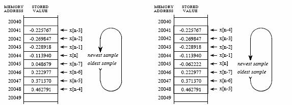
(a) (b)
Figure 3‑4: Circular buffer operation. a. Circular buffer at some instant and b. Circular buffer after next sample.
In real-time processing, the output signal is produced at the same time that the input signal is being acquired. For example, this is needed in telephone communication, hearing aids, and radar. These applications must have the information immediately available, although it can be delayed by a short amount. For instance, a 10-millisecond delay in a telephone call cannot be detected by the speaker or listener. Likewise, it makes no difference if a radar signal is delayed by a few seconds before being displayed to the operator. Real-time applications input a sample, perform the algorithm, and output a sample, over-and-over. Alternatively, they may input a group of samples, perform the algorithm, and output a group of samples. This is the world of Digital Signal Processors.
Now imagine that the FIR filter in Figure 3‑2 being implemented in real-time. To calculate the output sample, we must have access to a certain number of the most recent samples from the input. For example, suppose we use eight coefficients in this filter. This means we must know the value of the eight most recent samples from the input signal. These eight samples must be stored in memory and continually updated as new samples are acquired. What is the best way to manage these stored samples? The answer is circular buffering. Figure 3‑4 illustrates an eight sample circular buffer. We have placed this circular buffer in eight consecutive memory locations, 20041 to 20048. Figure 3‑4 (a) shows how the eight samples from the input might be stored at one particular instant in time, while (b) shows the changes after the next sample is acquired. The idea of circular buffering is that the end of this linear array is connected to its beginning; memory location 20041 is viewed as being next to 20048, just as 20044 is next to 20045. You keep track of the array by a pointer that indicates where the most recent sample resides. For instance, in (a) the pointer contains the address 20044, while in (b) it contains 20045. When a new sample is acquired, it replaces the oldest sample in the array, and the pointer is moved one address ahead. Circular buffers are efficient because only one value needs to be changed when a new sample is acquired.
3.2.2 Mathematics
To perform the simple arithmetic required, DSP processors need special high-speed arithmetic units. Most DSP operations require additions and multiplications together. So DSP processors usually have hardware adders and multipliers which can be used in parallel within a single instruction. Figure 3‑5 shows the data path for the Lucent DSP32C processor. The hardware multiply and add work in parallel so that in the space of a single instruction, both an add and a multiply can be completed.
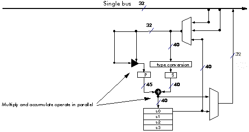
Figure 3‑5: The data path for the Lucent DSP32C processor.
Delays require that intermediate values be held for later use. This may also be a requirement, for example, when keeping a running total - the total can be kept within the processor to avoid wasting repeated reads from and writes to memory. For this reason DSP processors have lots of registers which can be used to hold intermediate values. Registers may be fixed point or floating point format.
Array handling requires that data can be fetched efficiently from consecutive memory locations. This involves generating the next required memory address. For this reason DSP processors have address registers which are used to hold addresses and can be used to generate the next needed address efficiently:
The ability to generate new addresses efficiently is a characteristic feature of DSP processors. Usually, the next needed address can be generated during the data fetch or store operation, and with no overhead. DSP processors have rich sets of address generation operations.
|
*rP |
register indirect |
Read the data pointed to by the address in register rP |
|
*rP++ |
post increment |
Having read the data, post increment the address pointer to point to the next value in the array |
|
*rP-- |
post decrement |
Having read the data, post decrement the address pointer to point to the previous value in the array |
|
*rP++rI |
register post increment |
Having read the data, post increment the address pointer by the amount held in register rI to point to rI values further down the array |
|
*rP++rIr |
bit reversed |
Having read the data, post increment the address pointer to point to the next value in the array, as if the address bits were in bit reversed order |
Figure 3‑6: Addressing modes for the Lucent DSP32C processor.
Figure 3‑6 shows some addressing modes for the Lucent DSP32C processor. The assembler syntax is very similar to C language. Whenever an operand is fetched from memory using register indirect addressing, the address register can be incremented to point to the next needed value in the array. This address increment is free - there is no overhead involved in the address calculation - and in the case of the Lucent DSP32C, processor up to three such addresses may be generated in each single instruction. Address generation is an important factor in the speed of DSP processors at their specialized operations.
The last addressing mode - bit reversed - shows how specialized DSP processors can be. Bit reversed addressing arises when a table of values has to be reordered by reversing the order of the address bits:
- reverse the order of the bits in each address
- shuffle the data so that the new, bit reversed, addresses are in ascending order
This operation is required in the Fast Fourier Transform - and just about nowhere else. So one can see that DSP processors are designed specifically to calculate the Fast Fourier Transform efficiently.
3.2.3 Input and Output Interfaces
In addition to the mathematics, in practice DSP is mostly dealing with the real world. Although this aspect is often forgotten, it is of great importance and marks some of the greatest distinctions between DSP processors and general-purpose microprocessors.
In a typical DSP application, the processor will have to deal with multiple sources of data from the real world (Figure 3‑7). In each case, the processor may have to be able to receive and transmit data in real time, without interrupting its internal mathematical operations. There are three sources of data from the real world:
- Signals coming in and going out
- Communication with an overall system controller of a different type
- Communication with other DSP processors of the same type
These multiple communications routes mark the most important distinctions between DSP processors and general-purpose processors. The need to deal with these different sources of data efficiently leads to special communication features on DSP processors:
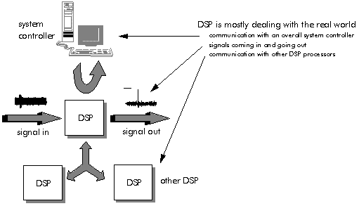
Figure 3‑7: Communication of DSP with overall system controllers.
When DSP processors first came out, they were rather fast processors: for example the first floating point DSP - the AT&T DSP32 - ran at 16 MHz at a time when PC computer clocks were 5 MHz. This meant that we had very fast floating point processors: a fashionable demonstration at the time was to plug a DSP board into a PC and run a fractal (Mandelbrot) calculation on the DSP and on a PC side by side. The DSP fractal was of course faster. Today, however, the fastest DSP processor is the Texas TMS320C6201, which runs at 200 MHz. This is no longer very fast compared with an entry level PC. In addition, the same fractal today will actually run faster on the PC than on the DSP. However, DSP processors are still used - why? The answer lies only partly in that the DSP can run several operations in parallel: a far more basic answer is that the DSP can handle signals very much better than a Pentium. Try feeding eight channels of high quality audio data in and out of a Pentium simultaneously in real time, without affecting the processor performance, if you want to see a real difference.
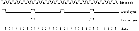
Figure 3‑8: The four activities on a synchronous serial port.
Signals tend to be fairly continuous, but at audio rates or not much higher. They are usually handled by high-speed synchronous serial ports. Serial ports are inexpensive - having only two or three wires - and are well suited to audio or telecommunications data rates up to 10 Mbit/s. Most modern speech and audio analogue to digital converters interface to DSP serial ports with no intervening logic. A synchronous serial port requires only three wires: clock, data, and word sync (Figure 3‑8). The addition of a fourth wire (frame sync) and a high impedance state when not transmitting makes the port capable of Time Division Multiplex (TDM) data handling, which is ideal for telecommunications:
DSP processors usually have synchronous serial ports - transmitting clock and data separately - although some, such as the Motorola DSP56000 family, have asynchronous serial ports as well (where the clock is recovered from the data). Timing is versatile, with options to generate the serial clock from the DSP chip clock or from an external source. The serial ports may also be able to support separate clocks for receive and transmit - a useful feature, for example, in satellite modems where the clocks are affected by Doppler shifts. Most DSP processors also support companding to A-law or mu-law in serial port hardware with no overhead - the Analog Devices ADSP2181 and the Motorola DSP56000 family does this in the serial port, whereas the Lucent DSP32C has a hardware compander in its data path instead.
The serial port will usually operate under DMA - data presented at the port is automatically written into DSP memory without stopping the DSP - with or without interrupts. It is usually possible to receive and transmit data simultaneously.
The serial port has dedicated instructions which make it simple to handle. Because it is standard to the chip, this means that many types of actual I/O hardware can be supported with little or no change to code - the DSP program simply deals with the serial port, no matter to what I/O hardware this is attached.
Host communications is an element of many, though not all, DSP systems. Many systems will have another, general purpose, processor to supervise the DSP: for example, the DSP might be on a PC plug-in card or a VME card - simpler systems might have a microcontroller to perform a 'watchdog' function or to initialize the DSP on power up. Whereas signals tend to be continuous, host communication tends to require data transfer in batches - for instance to download a new program or to update filter coefficients. Some DSP processors have dedicated host ports which are designed to communicate with another processor of a different type, or with a standard bus. For instance the Lucent DSP32C has a host port which is effectively an 8 bit or 16 bit ISA bus: the Motorola DSP56301 and the Analog Devices ADSP21060 have host ports which implement the PCI bus.
The host port will usually operate under DMA - data presented at the port is automatically written into DSP memory without stopping the DSP - with or without interrupts. It is usually possible to receive and transmit data simultaneously.
The host port has dedicated instructions, which make it simple to handle. The host port imposes a welcome element of standardization to plug-in DSP boards - because it is standard to the chip, it is relatively difficult for individual designers to make the bus interface different. For example, of the 22 main different manufacturers of PC plug-in cards using the Lucent DSP32C, 21 are supported by the same PC interface code: this means it is possible to swap between different cards for different purposes, or to change to a cheaper manufacturer, without changing the PC side of the code. Of course this is not foolproof - some engineers will always 'improve upon' a standard by making something incompatible if they can - but at least it limits unwanted creativity.
Interprocessor communications is needed when a DSP application is too much for a single processor - or where many processors are needed to handle multiple but connected data streams. Link ports provide a simple means to connect several DSP processors of the same type. The Texas TMS320C40 and the Analog Devices ADSP21060 both have six link ports (called 'comm. ports' for the 'C40). These would ideally be parallel ports at the word length of the processor, but this would use up too many pins (six ports each 32 bits wide=192, which is a lot of pins even if we neglect grounds). So a hybrid called serial/parallel is used: in the 'C40, comm. ports are 8 bits wide and it takes four transfers to move one 32 bit word - in the 21060, link ports are 4 bits wide and it takes 8 transfers to move one 32 bit word.
The link port will usually operate under DMA - data presented at the port is automatically written into DSP memory without stopping the DSP - with or without interrupts. It is usually possible to receive and transmit data simultaneously. This is a lot of data movement - for example the Texas TMS320C40 could in principle use all its six comm. ports at their full rate of 20 MByte/s to achieve data transfer rates of 120 MByte/s. In practice, of course, such rates exist only in the dreams of marketing men since other factors such as internal bus bandwidth come into play.
The link ports have dedicated instructions which make them simple to handle. Although they are sometimes used for signal I/O, this is not always a good idea since it involves very high speed signals over many pins and it can be hard for external hardware to exactly meet the timing requirements.
3.2.4 Architecture of the DSP
One of the biggest bottlenecks in executing DSP algorithms is transferring information to and from memory. This includes data, such as samples from the input signal and the filter coefficients, as well as program instructions, the binary codes that go into the program sequencer. For example, suppose we need to multiply two numbers that reside somewhere in memory. To do this, we must fetch three binary values from memory, the numbers to be multiplied, plus the program instruction describing what to do. To fetch the two operands in a single instruction cycle, we need to be able to make two memory accesses simultaneously. Actually, since we also need to store the result - and to read the instruction itself - we really need more than two memory accesses per instruction cycle.
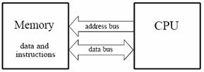
Figure 3‑9: The Von Neumann architecture uses a single memory to hold both data and instructions.
Figure 3‑9 shows how this seemingly simple task is done in a traditional microprocessor. This is often called Von Neumann architecture. Von Neumann architecture contains a single memory and a single bus for transferring data into and out of the central processing unit (CPU). Multiplying two numbers requires at least three clock cycles, one to transfer each of the three numbers over the bus from the memory to the CPU. We don't count the time to transfer the result back to memory, because we assume that it remains in the CPU for additional manipulation (such as the sum of products in an FIR filter). Since the von Neumann architecture uses only a single memory bus, it is cheap, requiring less pins, and simple to use because the programmer can place instructions or data anywhere throughout the available memory. But it does not permit multiple memory accesses.
The modified von Neumann architecture allows multiple memory accesses per instruction cycle by the simple trick of running the memory clock faster than the instruction cycle. For example the Lucent DSP32C runs with an 80 MHz clock: this is divided by four to give 20 million instructions per second (MIPS), but the memory clock runs at the full 80 MHz - each instruction cycle is divided into four 'machine states' and a memory access can be made in each machine state, permitting a total of four memory accesses per instruction cycle (Figure 3‑10). In this case the modified von Neumann architecture permits all the memory accesses needed to support addition or multiplication: fetch of the instruction; fetch of the two operands; and storage of the result.
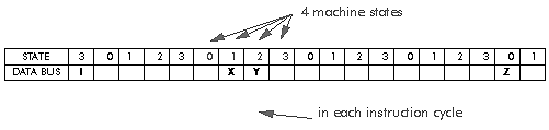
Figure 3‑10: Multiple memory accesses per instruction cycle in modified von Neumann architecture. Four memory accesses per instruction cycle.
The Von Neumann design is quite satisfactory when you are content to execute all of the required tasks in serial. In fact, most computers today are of the Von Neumann design. We only need other architectures when very fast processing is required, and we are willing to pay the price of increased complexity. This leads us to the Harvard architecture, shown Figure 3‑11. This is named for the work done at Harvard University in the 1940s under the leadership of Howard Aiken (1900-1973). As shown in this illustration, Aiken insisted on separate memories for data and program instructions, with separate buses for each. Since the buses operate independently, program instructions and data can be fetched at the same time, improving the speed over the single bus design. Most present day DSPs use this dual bus architecture.
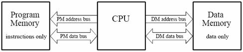
Figure 3‑11: The Harvard architecture uses separate memories for data and instructions, providing higher speed.
The Harvard architecture has two separate physical memory buses. This allows two simultaneous memory accesses. The true Harvard architecture dedicates one bus for fetching instructions, with the other available to fetch operands. This is inadequate for DSP operations, which usually involve at least two operands. So DSP Harvard architectures usually permit the program bus to be used also for access of operands. Note that it is often necessary to fetch three things - the instruction plus two operands - and the Harvard architecture is inadequate to support this.
The Harvard architecture requires two memory buses. This makes it expensive to bring off the chip - for example a DSP using 32 bit words and with a 32 bit address space requires at least 64 pins for each memory bus - a total of 128 pins if the Harvard architecture is brought off the chip. This results in very large chips, which are difficult to design into a circuit.
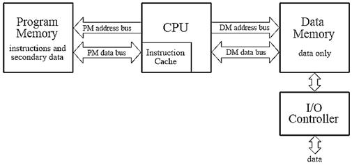
Figure 3‑12: The Super Harvard Architecture improves upon the Harvard design by adding an instruction cache and a dedicated I/O controller.
Figure 3‑12 illustrates the next level of sophistication, the Super Harvard Architecture. This term was coined by Analog Devices to describe the The Scientist and Engineer's Guide to Digital Signal Processing 510 internal operation of their ADSP-2106x and new ADSP-211xx families of Digital Signal Processors. These are called SHARC® DSPs, a contraction of the longer term, Super Harvard Architecture. The idea is to build upon the Harvard architecture by adding features to improve the throughput. While the SHARC DSPs are optimized in dozens of ways, two areas are important enough to be included in Figure 3‑12: an instruction cache, and an I/O controller. First, let's look at how the instruction cache improves the performance of the Harvard architecture. A handicap of the basic Harvard design is that the data memory bus is busier than the program memory bus. When two numbers are multiplied, two binary values (the numbers) must be passed over the data memory bus, while only one binary value (the program instruction) is passed over the program memory bus. To improve upon this situation, we start by relocating part of the "data" to program memory. For instance, we might place the filter coefficients in program memory, while keeping the input signal in data memory. (This relocated data is called "secondary data" in the illustration).
At first glance, this doesn't seem to help the situation; now we must transfer one value over the data memory bus (the input signal sample), but two values over the program memory bus (the program instruction and the coefficient). In fact, if we were executing random instructions, this situation would be no better at all.
However, DSP algorithms generally spend most of their execution time in loops. This means that the same set of program instructions will continually pass from program memory to the CPU. The Super Harvard architecture takes advantage of this situation by including an instruction cache in the CPU. This is a small memory that contains about 32 of the most recent program instructions. The first time through a loop, the program instructions must be passed over the program memory bus. This results in slower operation because of the conflict with the coefficients that must also be fetched along this path. However, on additional executions of the loop, the program instructions can be pulled from the instruction cache. This means that all of the memory to CPU information transfers can be accomplished in a single cycle: the sample from the input signal comes over the data memory bus, the coefficient comes over the program memory bus, and the program instruction comes from the instruction cache. In the jargon of the field, this efficient transfer of data is called a high memory access bandwidth.
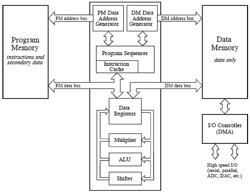
Figure 3‑13: Typical DSP architecture. Digital Signal Processors are designed to implement tasks in parallel. This simplified diagram is the Analog Devices SHARC DSP.
Figure 3‑13 presents a more detailed view of the SHARC architecture, showing the I/O controller connected to data memory. This is how the signals enter and exit the system. For instance, the SHARC DSPs provides both serial and parallel communications ports. These are extremely high speed connections. For example, at a 40 MHz clock speed, there are two serial ports that operate at 40 MBits/second each, while six parallel ports each provide a 40 Mbytes/second data transfer. When all six parallel ports are used together, the data transfer rate is an incredible 240 Mbytes/second.
Both Harvard and von Neuman architectures require the programmer to be careful of where in memory data is placed: for example with the Harvard architecture, if both needed operands are in the same memory bank then they cannot be accessed simultaneously.
3.2.5 Data formats in DSP processors
DSP processors store data in fixed or floating point formats. It is worth noting that fixed point format is not quite the same as integer (Figure 3‑14). The integer format is straightforward: representing whole numbers from 0 up to the largest whole number that can be represented with the available number of bits. Fixed point format is used to represent numbers that lie between 0 and 1, with a binary point assumed to lie just after the most significant bit. The most significant bit in both cases carries the sign of the number. The size of the fraction represented by the smallest bit is the precision of the fixed point format. The size of the largest number that can be represented in the available word length is the dynamic range of the fixed point format.
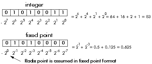
Figure 3‑14: The comparison integer and fixed point data formats.
To make the best use of the full available word length in the fixed point format, the programmer has to make some decisions. If a fixed point number becomes too large for the available word length, the programmer has to scale the number down, by shifting it to the right: in the process lower bits may drop off the end and be lost. If a fixed point number is small, the number of bits actually used to represent it is small. The programmer may decide to scale the number up, in order to use more of the available word length. In both cases the programmer has to keep a track of by how much the binary point has been shifted, in order to restore all numbers to the same scale at some later stage.
Floating point format has the remarkable property of automatically scaling all numbers by moving, and keeping track of, the binary point so that all numbers use the full word length available but never overflow.
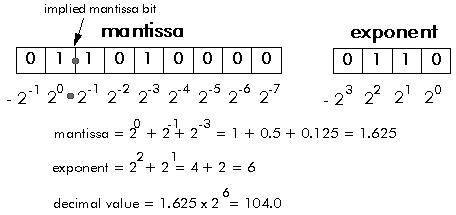
Figure 3‑15: The floating point format.
Floating point numbers have two parts: the mantissa, which is similar to the fixed point part of the number, and an exponent which is used to keep track of how the binary point is shifted (Figure 3‑15). Every number is scaled by the floating point hardware. If a number becomes too large for the available word length, the hardware automatically scales it down, by shifting it to the right. If a number is small, the hardware automatically scales it up, in order to use the full available word length of the mantissa. In both cases the exponent is used to count how many times the number has been shifted. In floating point numbers the binary point comes after the second most significant bit in the mantissa.
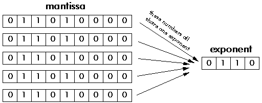
Figure 3‑16: The block floating point format.
The block floating point format in Figure 3‑16 provides some of the benefits of floating point, but by scaling blocks of numbers rather than each individual number. Block floating point numbers are actually represented by the full word length of a fixed point format. If any one of a block of numbers becomes too large for the available word length, the programmer scales down all the numbers in the block, by shifting them to the right. If the largest of a block of numbers is small, the programmer scales up all numbers in the block, in order to use the full available word length of the mantissa. In both cases the exponent is used to count how many times the numbers in the block have been shifted.
Some specialized processors, such as those from Zilog, have special features to support the use of block floating point format. More usually, it is up to the programmer to test each block of numbers and carry out the necessary scaling.
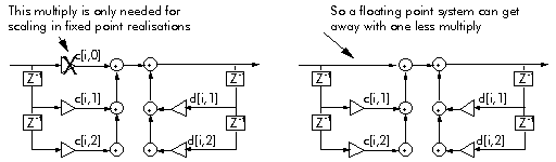
Figure 3‑17: The advantage of floating point format over fixed point. Floating point hardware automatically scales every number to avoid overflow.
The floating point format has one further advantage over fixed point: it is faster. Because of quantization error, a basic direct form 1 IIR filter second order section requires an extra multiplier, to scale numbers and avoid overflow. But the floating point hardware automatically scales every number to avoid overflow, so this extra multiplier is not required (Figure 3‑17).
3.2.6 Precision and dynamic range
The precision with which numbers can be represented is determined by the word length in the fixed point format, and by the number of bits in the mantissa in the floating point format. In a 32 bit DSP processor the mantissa is usually 24 bits, so the precision of a floating point DSP is the same as that of a 24 bit fixed point processor. But floating point has one further advantage over fixed point: because the hardware automatically scales each number to use the full word length of the mantissa, the full precision is maintained even for small numbers (Figure 3‑18).
There is a potential disadvantage to the way floating point works. Because the hardware automatically scales and normalizes every number, the errors due to truncation and rounding depend on the size of the number. If we regard these errors as a source of quantization noise, then the noise floor is modulated by the size of the signal. Although the modulation can be shown to be always downwards (that is, a 32 bit floating point format always has noise which is less than that of a 24 bit fixed point format), the signal dependent modulation of the noise may be undesirable, notably, the audio industry prefers to use 24 bit fixed point DSP processors over floating point because it is thought by some that the floating point noise floor modulation is audible. The precision directly affects quantization error.
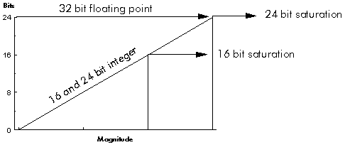
Figure 3‑18: The floating point hardware automatically scales each number and the full precision is maintained even for small numbers
The largest number which can be represented determines the dynamic range of the data format. In fixed point format this is straightforward: the dynamic range is the range of numbers that can be represented in the available word length. For floating point format, though, the binary point is moved automatically to accommodate larger numbers, so the dynamic range is determined by the size of the exponent. Therefore the dynamic range of a floating point format is enormously larger than for a fixed point format (Figure 3‑19).
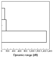
Figure 3‑19: The dynamic range comparison of floating point format over fixed point.
While the dynamic range of a 32 bit floating point format is large, it is not infinite, thus it is possible to suffer overflow and underflow even with a 32 bit floating point format. A classic example of this can be seen by running fractal (Mandelbrot) calculations on a 32 bit DSP processor. After quite a long time, the fractal pattern ceases to change because the increment size has become too small for a 32 bit floating point format to represent.
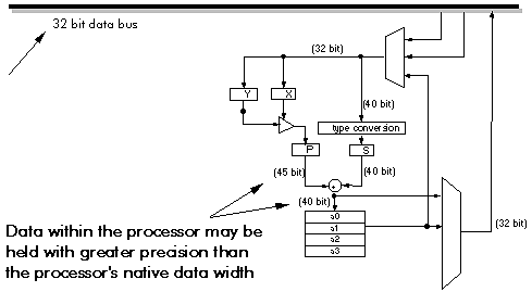
Figure 3‑20: The data path of the Lucent DSP32C
Most DSP processors have extended precision registers within the processor. Figure 3‑20 shows the data path of the Lucent DSP32C processor. Although this is a 32 bit floating point processor, it uses 40 and 45 bit registers internally, thus, results can be held to a wider dynamic range internally than when written to memory.